 English
- English
-
 Español
 -
 Português
 -
 русский
 -
 Français
 -
 日本語
日本語 -
 Deutsch
 -
 tiếng Việt
 -
 Italiano
 -
 Nederlands
 -
 ภาษาไทย
 -
 Polski
 -
 한국어
한국어 -
 Svenska
 -
 magyar
 -
 Malay
Malay -
 বাংলা ভাষার
 -
 Dansk
Dansk -
 Suomi
Suomi -
 हिन्दी
 -
 Pilipino
 -
 Türkçe
 -
 Gaeilge
 -
 العربية
 -
 Indonesia
 -
 Norsk
Norsk -
 تمل
تمل -
 český
český -
 ελληνικά
 -
 український
 -
 Javanese
 -
 فارسی
فارسی -
 தமிழ்
தமிழ் -
 తెలుగు
 -
 नेपाली
 -
 Burmese
 -
 български
 -
 ລາວ
ລາວ -
 Latine
 -
 Қазақша
 -
 Euskal
 -
 Azərbaycan
 -
 Slovenský jazyk
 -
 Македонски
 -
 Lietuvos
 -
 Eesti Keel
 -
 Română
 -
 Slovenski


How to solve the problem of tin beads generated during PCB production
2024-06-22
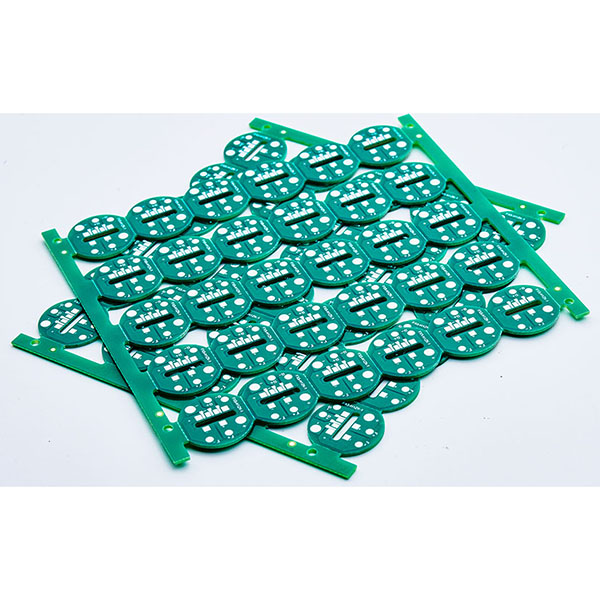
There are many problems with PCB circuit boards during production, among which short circuit failure caused by tin beads is always hard to guard against. Tin beads refer to spherical particles of different sizes formed when the solder paste leaves the PCB solder end during the reflow soldering process and solidifies instead of gathering on the pad. Tin beads produced during reflow soldering mainly appear on the sides between the two ends of rectangular chip components or between fine-pitch pins. Tin beads not only affect the appearance of the product, but more importantly, due to the density of PCBA processed components, there is a risk of short circuit during use, thus affecting the quality of electronic products. As a PCB circuit board manufacturer, there are many ways to solve this problem. Should we improve production, improve the process, or optimize from the source of design?
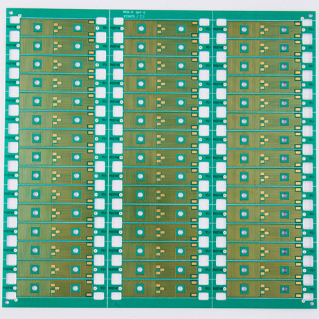
Causes of tin beads
1. From the design perspective, the PCB pad design is unreasonable, and the grounding pad of the special package device extends too far beyond the device pin
2. The reflow temperature curve is improperly set. If the temperature in the preheating zone rises too fast, the moisture and solvent inside the solder paste will not be completely volatilized, and the moisture and solvent will boil when reaching the reflow zone, splashing the solder paste to form tin beads.
3. Improper steel mesh opening design structure. If solder balls always appear in the same position, it is necessary to check the steel mesh opening structure. The steel mesh causes missed printing and unclear printed outlines, bridging each other, and a large number of tin beads will inevitably be generated after reflow soldering.
4. The time between the completion of the patch processing and the reflow soldering is too long. If the time from patch to reflow soldering is too long, the solder particles in the solder paste will oxidize and deteriorate, and the activity will decrease, which will cause the solder paste to not reflow and produce tin beads.
5. When patching, the z-axis pressure of the patch machine causes the solder paste to be squeezed out of the pad at the moment the component is attached to the PCB, which will also cause the formation of tin beads after welding.
6. Insufficient cleaning of PCBs with incorrectly printed solder paste leaves solder paste on the surface of the PCB and in the through holes, which is also the cause of solder balls.
7. During the component mounting process, solder paste is placed between the pins and pads of chip components. If the pads and component pins are not well wetted, some liquid solder will flow out of the weld to form solder beads.
Specific solution:
During the DFA review, the package size and the pad design size are checked for matching, mainly considering reducing the amount of tinning at the bottom of the component, thereby reducing the probability of solder paste extruding the pad.
Solving the tin bead problem by optimizing the stencil opening size is a fast and efficient solution. The shape and size of the stencil opening are summarized. Point-to-point analysis and optimization should be carried out according to the poor phenomenon of the solder joints. According to actual problems, continuous experience is summarized for optimization and tinning. It is very important to standardize the management of the stencil opening design, otherwise it will directly affect the production pass rate.
Optimizing the reflow oven temperature curve, machine mounting pressure, workshop environment and reheating and stirring of solder paste before printing is also an important means to solve the tin bead problem.


X
We use cookies to offer you a better browsing experience, analyze site traffic and personalize content. By using this site, you agree to our use of cookies.
Privacy Policy