 English
- English
-
 Español
 -
 Português
 -
 русский
 -
 Français
 -
 日本語
日本語 -
 Deutsch
 -
 tiếng Việt
 -
 Italiano
 -
 Nederlands
 -
 ภาษาไทย
 -
 Polski
 -
 한국어
한국어 -
 Svenska
 -
 magyar
 -
 Malay
Malay -
 বাংলা ভাষার
 -
 Dansk
Dansk -
 Suomi
Suomi -
 हिन्दी
 -
 Pilipino
 -
 Türkçe
 -
 Gaeilge
 -
 العربية
 -
 Indonesia
 -
 Norsk
Norsk -
 تمل
تمل -
 český
český -
 ελληνικά
 -
 український
 -
 Javanese
 -
 فارسی
فارسی -
 தமிழ்
தமிழ் -
 తెలుగు
 -
 नेपाली
 -
 Burmese
 -
 български
 -
 ລາວ
ລາວ -
 Latine
 -
 Қазақша
 -
 Euskal
 -
 Azərbaycan
 -
 Slovenský jazyk
 -
 Македонски
 -
 Lietuvos
 -
 Eesti Keel
 -
 Română
 -
 Slovenski


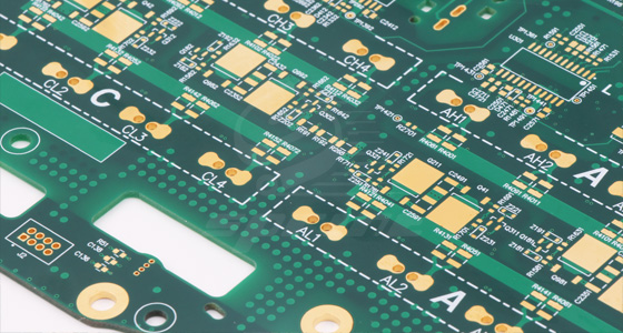
Explore the application of multi-layer PCB in complex electronic devices
2024-10-21
With the rapid development of electronic technology, electronic devices are becoming more and more complex and feature-rich. In this context, multi-layer circuit boards have become one of the key technologies for realizing these complex electronic devices due to their excellent performance and compact design. The following will explore the application of multi-layer PCB boards in complex electronic devices and the advantages they bring.
1. Application Examples of Multilayer PCB in Complex Electronic Equipment
Aerospace Field
In aerospace equipment, multilayer PCB are used to achieve high-density electronic system integration while ensuring reliability and performance in extreme environments.
Medical Equipment
Multilayer PCB are used in medical equipment to achieve high-precision signal processing and control while meeting strict safety and hygiene standards.
High-Performance Computing
In the field of high-performance computing, multilayer PCB are used to build complex processor and memory arrays to achieve high-speed data processing.
Communication Equipment
Multilayer PCB are used in communication equipment to achieve high-speed data transmission and signal processing while keeping the equipment compact and lightweight.
2. Advantages of multi-layer PCB
Improve signal integrity
Multi-layer PCB can provide shorter signal paths and better signal shielding, thereby reducing interference and attenuation in signal transmission and improving signal integrity.
Enhance electromagnetic compatibility
The design of multi-layer PCB can manage electromagnetic interference (EMI) more effectively, reducing mutual interference between devices through ground planes and shielding layers.
Optimize thermal management
Multi-layer PCB can design more complex thermal management solutions, such as using thermally conductive materials or burying heat pipes to improve the heat dissipation efficiency of the device.
Save space
Multi-layer PCB allow more electronic components to be integrated in a smaller space, which is especially important for portable devices and compact systems.
3. Challenges in the design and manufacture of multi-layer PCB
Design complexity
The design of multi-layer PCB needs to consider more factors, such as signal routing, power distribution, thermal management, etc., which increases the complexity of the design.
Manufacturing precision
The manufacturing of multi-layer PCB requires higher precision and more advanced processes to ensure the quality and performance of the circuit.
Cost control
Since the design and manufacturing process of multi-layer PCB is more complex, cost control becomes an important consideration.
The use of multilayer PCB is becoming more and more common in modern electronic devices, especially those that require high performance, high reliability and compact design. Multilayer PCB greatly improve the integration and performance of electronic devices by arranging circuits on multiple levels. The application of multilayer PCB in complex electronic devices is becoming more and more extensive, and they provide the possibility of achieving high performance, high reliability and compact design of electronic systems. Although there are many challenges in designing and manufacturing multilayer PCB, these challenges are gradually being overcome with the advancement and innovation of technology. In the future, multilayer PCB will continue to play a key role in promoting the development of electronic devices.


X
We use cookies to offer you a better browsing experience, analyze site traffic and personalize content. By using this site, you agree to our use of cookies.
Privacy Policy