 English
-
 English
 -
 Español
 -
 Português
 -
 русский
 -
 Français
 -
 日本語
日本語 -
 Deutsch
 -
 tiếng Việt
 -
 Italiano
 -
 Nederlands
 -
 ภาษาไทย
 -
 Polski
 -
 한국어
한국어 -
 Svenska
 -
 magyar
 -
 Malay
Malay -
 বাংলা ভাষার
 -
 Dansk
Dansk -
 Suomi
Suomi -
 हिन्दी
 -
 Pilipino
 -
 Türkçe
 -
 Gaeilge
 -
 العربية
 -
 Indonesia
 -
 Norsk
Norsk -
 تمل
تمل -
 český
český -
 ελληνικά
 -
 український
 -
 Javanese
 -
 فارسی
فارسی -
 தமிழ்
தமிழ் -
 తెలుగు
 -
 नेपाली
 -
 Burmese
 -
 български
 -
 ລາວ
ລາວ -
 Latine
 -
 Қазақша
 -
 Euskal
 -
 Azərbaycan
 -
 Slovenský jazyk
 -
 Македонски
 -
 Lietuvos
 -
 Eesti Keel
 -
 Română
 -
 Slovenski
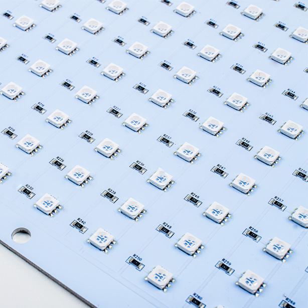
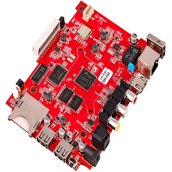
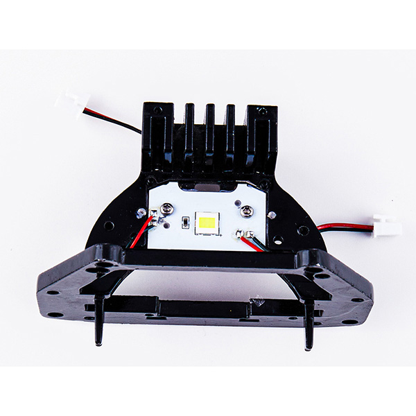
SMT Assembly
You can rest assured to buy Jiubao SMT Assembly from our factory. As our lives become more and more inseparable from electronic products, the widespread use of electronic products has led more and more companies to join the electronic product industry.
Send Inquiry
Product Description
SMT Assembly
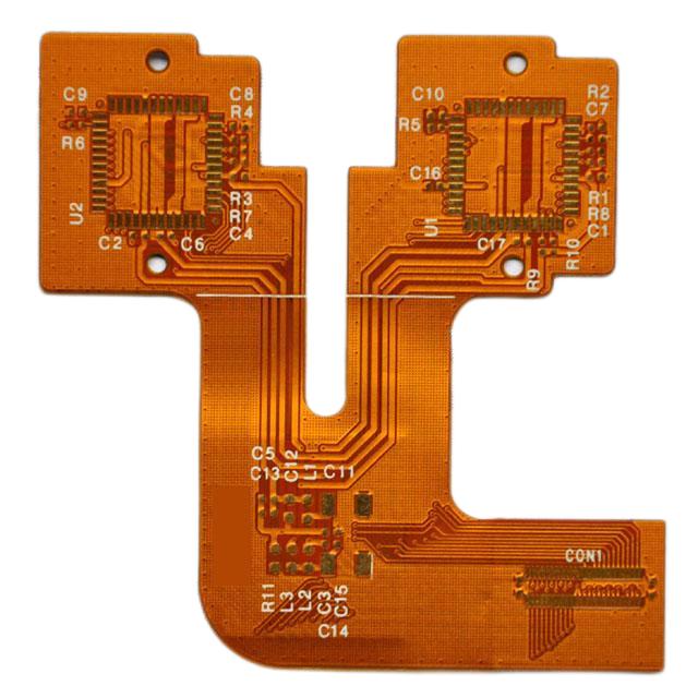
You can rest assured to buy Jiubao SMT Assembly from our factory. As our lives become more and more inseparable from electronic products, the widespread use of electronic products has led more and more companies to join the electronic product industry. To make electronic products, SMT chip processing is first of all inseparable.
What is SMT Technology?
Surface Mounted Technology referred to as SMT.
SMT patch is actually a series of PCB-based processing.
SMT is a surface mount technology, which is a popular technology and process in the electronic assembly industry. SMT patch is based on PCB. First, the SMT soldering material solder paste is printed onto the pads of the PCB bare board. Then, the placement machine is used. The electronic components are mounted on the pads of the bare PCB board, and then the PCB board is sent to reflow soldering for soldering. The SMT patch is to mount the electronic components on the bare PCB board through a series of processes.
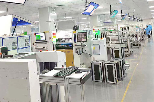
Why Use SMT?
Electronic products pursue miniaturization, small size, high assembly density and light weight. The volume and weight of SMD components are only about 1/10 of those of traditional plug-in components. Generally, after SMT is used, the volume of electronic products is reduced by 40%~60%, and the weight Reduce 60%~80%. The previously used perforated insert elements cannot be scaled down. The functions of electronic products need to be complete, and the integrated circuits (ICs) used have no perforated components, especially large-scale and highly integrated ICs, and surface mount technology has to be used. Product mass production, production automation, the factory must produce high-quality products at low cost and high yield to meet customer needs and strengthen market competitiveness, the development of electronic components, the development of integrated circuits (IC), and the multiple applications of semiconductor materials. The electronic technology revolution is imperative, JBPCB conforms to the international electronic product trend, from PCB to PCBA one-stop procurement service manufacturer.
Features of SMT:
High reliability and strong anti-vibration ability. Solder joint defect rate is low. Good high frequency characteristics. Electromagnetic and radio frequency interference is reduced.
It is easy to realize automation and improve production efficiency. Reduce costs by 30% to 50%. Save material, energy, equipment, manpower, time, etc.
It is easy to realize automation and improve production efficiency. Reduce costs by 30% to 50%. Save material, energy, equipment, manpower, time, etc.
SMT Chip Technology Process:
The SMT patch process is divided into: solder paste printing, SMT patch, intermediate inspection, reflow soldering, post-furnace inspection, performance testing, and rework. The following is shared by JBPCB in detail.
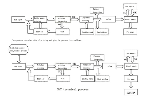
1. Solder paste printing by solder paste printer: its function is to leak solder paste or patch glue onto the pads of the PCB to prepare for the soldering of components. The equipment used is a solder paste printing machine, which is located at the forefront of the SMT production line.
2. Use a glue dispenser to dispense glue when using a double-sided patch panel: it drips glue onto the fixed position of the PCB, and its main function is to fix the components to the PCB board. The equipment used is a glue dispenser, which is located at the front end of the SMT production line or behind the inspection equipment.
3. Use a placement machine to mount components: its function is to accurately mount the surface-mounted components to the fixed position of the PCB. The equipment used is a placement machine, which is located behind the screen printing machine in the SMT production line.
4. Curing the patch glue: its function is to melt the patch glue, so that the surface-mounted components and the PCB board are firmly bonded together. The equipment used is a curing oven or reflow soldering, which is located behind the placement machine in the SMT production line.
5. Reflow soldering: Its function is to melt the solder paste, so that the surface mount components and the PCB board are firmly bonded together. The equipment used is a reflow oven, located behind the placement machine in the SMT production line.
6. Cleaning of the reflow soldered PCB: its function is to remove the soldering residues such as flux that are harmful to the human body on the assembled PCB board. The equipment used is a washing machine, the location may not be fixed, it may be online or not.
7. Inspection: Its function is to inspect the welding quality and assembly quality of the assembled PCB board. The equipment used includes magnifying glass, microscope, in-line tester (ICT), flying probe tester, automatic optical inspection (AOI), X-RAY inspection system, functional tester, etc. The location can be configured in a suitable place on the production line according to the needs of the inspection.
8. Rework: Its function is to rework the PCB board that has detected the failure. The tools used are soldering iron, rework station, etc. Configured anywhere in the production line.
What are the Three Important Processes in the SMT Process?
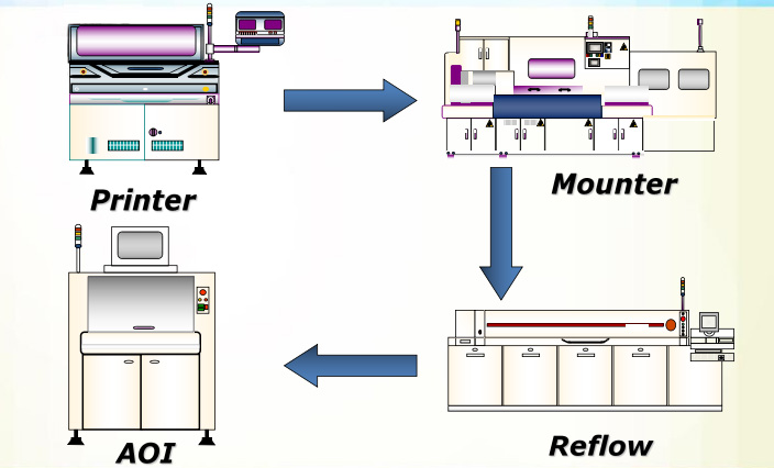
The three main steps in the SMT process are solder paste printing, component placement and reflow soldering.
When printing solder paste, first check whether the parameters of the solder paste printing machine are set correctly. The solder paste of the board should be on the solder pads, whether the height of the solder paste is set or in a "trapezoid" shape, and the edges of the solder paste should not have rounded corners or It collapses into a pile shape, but some peak shapes caused by pulling up some solder paste when the steel plate is detached are allowed. If the solder paste is not evenly distributed, it is necessary to check whether the solder paste on the scraper is insufficient or unevenly distributed. Also check the printed steel plate and other parameters. Finally, the solder paste should be shiny or damp under the microscope rather than dry.
Component placement Before placing components on the first board with solder paste, you should first confirm whether the material rack is properly placed, whether the components are correct, and whether the machine is in the correct position. After the first board is completed, it should be checked in detail that each part is correctly placed and lightly pressed in the center of the solder paste, rather than just "placed" on top of the solder paste. If you can see that the solder paste is slightly recessed under the microscope, it means that the placement is correct. This prevents the component from "slipping" during reflow. Need to confirm again whether the surface of the solder paste is still wet? If the board has been printed with solder paste for a long time, the solder paste will appear to have a dry and cracked surface. Such solder pastes can create "rosin solder joints" (RSJs) that cannot be inspected except after going through a reflow oven. This type of rosin solder joint is usually found in the assembly process of the through hole (Through Hole), which creates a thin transparent layer of rosin between the component and the pad, and blocks any electrical transmission. Last second check l Are all the components on the BOM (Bill Of Materials) consistent with the components on the board? l Are all positive and negative sensitive components such as diodes, tantalum capacitors and IC components placed in the correct direction?

Reflow oven: Once the reflow temperature curve is set (that is to say, many boards have been measured with thermocouples in advance and it is determined that there is no defect), only when there is a large change in quantity or a major defect occurs, the line to adjust the reflow profile. The so-called "perfect" solder joint means that the appearance is bright and smooth, and there is also a complete solder coating around the pin. Some oxides mixed with rosin residues can also be seen near the solder joints, which indicates that the flux has a cleaning function. This oxide is normal and usually detached from the PCB, but is also more likely to be detached from the pins on the component due to the cleaning effect of the flux, which also indicates that the component may have been stored for a period of time. A long time, even longer than a PCB. Old or incompletely mixed solder paste may produce small solder balls due to poor welding with solder pads or component pins (Note: Small solder balls may also be due to process defects such as There is moisture in the solder paste or the green paint (Soldermask) is defective). However, the poor welding condition may also be due to poor management, so that some boards have been touched by the hands of the staff, and the grease on the hands is left on the pads to cause the failure. Of course, this phenomenon may also be caused by too thin tin plating on the solder pads or component feet. Finally, to an inspector, a slightly grey solder joint may be caused by too old solder paste, too low reflow temperature, too short reflow time, or incorrectly set reflow profile, or reflow Welding furnace is malfunctioning. The small solder balls may be because the board has not been baked or has been baked for too long, or the component is too hot or the component is placed. Before entering the reflow oven, someone adjusted the component and squeezed out the solder paste. caused by outside the pads.
JB PCB-----one-stop Chinese PCB&PCB assembly manufacturer, from rapid prototyping to mass production, services include: PCB design + PCB production + component procurement + SMT assembly + plug-in assembly + BGA assembly + cable assembly + function Testing. We ensure 100% original and new components, never use defective or recycled parts.
Product quality is guaranteed. Fully compliant with ISO 9001 quality management system and IATF16949 certification, 100% fully tested before shipment.
The entire production process of JBPCB strictly implements 8 inspection procedures, and the defective rate of PCB assembly products is <0.2%. Our factory director has more than 30 years of experience in PCBA factory management. He has worked in many well-known factories and mastered various advanced management methods. The factory management team led by him can reasonably arrange production, flexibly allocate workers, easily deal with various abnormal production situations and emergencies, and ensure the smooth progress of production.
We ensure 100% original and brand new components and never use defective or recycled parts.
JB PCB has been deeply involved in the PCB industry for more than 12 years since 2010, and has rich manufacturing knowledge and experience to identify the quality of PCB boards. They have their own PCB and PCBA factories respectively, and their factories are world-renowned PCB&PCBA assembly one-stop service providers in terms of industry resources.
Therefore, customers can purchase PCB boards and PCBA together from us to reduce the overall procurement cost and shorten the overall procurement cycle.
FAQ
Q1: Are you a SMT PCB assembly supplier?
Yes, we are SMT PCB assembly manufacturer, we have advanced SMT machines, welcome to visit our factory in China.
Q2: Can we buy PCB components according to our requirements?
Yes, please send the specifications of PCB components to our mailbox: pcb@jbmcpcb.com, our staff will accurately match and find the components that are suitable for you.
Q3: Can I deliver from PCB design to PCBA?
Yes, we have professional engineers from PCB design, PCB manufacturing to PCBA assembly services. There are professional engineers to connect.
Hot Tags: SMT Assembly, China, Factory, Manufacturers, Suppliers, Price, Made in China
Send Inquiry
Please feel free to fill your inquiry in the form below. We will reply you in 24 hours.
Related Products
X
We use cookies to offer you a better browsing experience, analyze site traffic and personalize content. By using this site, you agree to our use of cookies.
Privacy Policy


